| CPC H01L 29/4966 (2013.01) [H01L 21/76838 (2013.01); H01L 21/76897 (2013.01); H01L 21/823437 (2013.01); H01L 29/41783 (2013.01); H01L 29/42376 (2013.01); H01L 29/66545 (2013.01)] | 17 Claims |
|
10. A gate structure, comprising:
a substrate divided into an N-type transistor region and a P-type transistor region;
an interlayer dielectric covering the substrate;
a first N-type gate structure disposed within the N-type transistor region, wherein the first N-type gate structure comprises:
a first trench embedded in the interlayer dielectric;
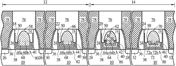
a first gate electrode disposed in the first trench, wherein the first gate electrode has a bullet-shaped profile under a cross-sectional view;
a gate dielectric layer contacting the first trench, wherein the gate dielectric layer is U-shaped, the gate dielectric layer has a first bottom and two sidewalls connecting to the first bottom, the two sidewalls are perpendicular to a top surface of the substrate, each of the two sidewalls has two different thicknesses, each of the two sidewalls has a step profile, and the gate dielectric layer has two ends which are lower than a top surface of the interlayer dielectric;
an N-type work function layer disposed between the gate dielectric layer and the first gate electrode, and the N-type work function layer contacting the first gate electrode;
a first P-type gate structure disposed within the P-type transistor region, wherein the first P-type gate structure comprises:
a second trench embedded in the interlayer dielectric;
a second gate electrode disposed in the second trench, wherein the second gate electrode has a first mushroom-shaped profile under a cross-sectional view;
the gate dielectric layer contacting the second trench;
the N-type work function layer disposed between the gate dielectric layer and the second gate electrode; and
a first P-type work function layer disposed between the gate dielectric layer and the N-type work function layer.
|