US 11,929,417 B2
Contacts for highly scaled transistors
Carlos H. Diaz, Los Altos Hills, CA (US); Chung-Cheng Wu, Hsin-Chu County (TW); Chia-Hao Chang, Hsinchu (TW); Chih-Hao Wang, Hsinchu County (TW); Jean-Pierre Colinge, Blot L'Eglise (FR); Chun-Hsiung Lin, Hsinchu County (TW); Wai-Yi Lien, Hsinchu (TW); and Ying-Keung Leung, Hsinchu (TW)
Assigned to TAIWAN SEMICONDUCTOR MANUFACTURING COMPANY, LTD., Hsinchu (TW)
Filed by Taiwan Semiconductor Manufacturing Company, Ltd., Hsinchu (TW)
Filed on Jun. 30, 2022, as Appl. No. 17/854,354.
Application 17/694,043 is a division of application No. 16/681,927, filed on Nov. 13, 2019, granted, now 11,276,763, issued on Mar. 15, 2022.
Application 15/362,470 is a division of application No. 14/872,673, filed on Oct. 1, 2015, granted, now 9,508,858, issued on Nov. 29, 2016.
Application 17/854,354 is a continuation of application No. 17/694,043, filed on Mar. 14, 2022.
Application 16/681,927 is a continuation of application No. 15/933,560, filed on Mar. 23, 2018, granted, now 10,497,792, issued on Dec. 3, 2019.
Application 15/933,560 is a continuation of application No. 15/362,470, filed on Nov. 28, 2016, granted, now 9,941,374, issued on Apr. 10, 2018.
Claims priority of provisional application 62/081,348, filed on Nov. 18, 2014.
Prior Publication US 2022/0328644 A1, Oct. 13, 2022
This patent is subject to a terminal disclaimer.
Int. Cl. H01L 29/94 (2006.01); H01L 21/768 (2006.01); H01L 23/522 (2006.01); H01L 23/528 (2006.01); H01L 23/532 (2006.01); H01L 29/417 (2006.01); H01L 29/423 (2006.01); H01L 29/45 (2006.01); H01L 29/66 (2006.01); H01L 29/76 (2006.01); H01L 29/775 (2006.01); H01L 29/78 (2006.01); H01L 29/786 (2006.01)
CPC H01L 29/45 (2013.01) [H01L 21/76852 (2013.01); H01L 23/5226 (2013.01); H01L 23/5283 (2013.01); H01L 23/53271 (2013.01); H01L 29/41733 (2013.01); H01L 29/41741 (2013.01); H01L 29/41791 (2013.01); H01L 29/42392 (2013.01); H01L 29/66666 (2013.01); H01L 29/775 (2013.01); H01L 29/785 (2013.01); H01L 29/78618 (2013.01); H01L 29/78642 (2013.01); H01L 29/78696 (2013.01); H01L 29/7827 (2013.01); H01L 29/7853 (2013.01); H01L 2029/7858 (2013.01)] 20 Claims
OG exemplary drawing
 
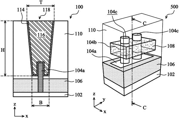
1. A device structure, comprising:
a semiconductor mesa;
a fin extending from the semiconductor mesa and comprising a lower portion, a middle portion over the lower portion, and an upper portion over the middle portion;
a metal gate structure engaging sidewalls of the middle portion of the fin; and
an interlayer dielectric (ILD) layer wrap around the metal gate structure, the upper portion, and the lower portion.