| CPC H01L 29/41791 (2013.01) [H01L 21/28518 (2013.01); H01L 21/823814 (2013.01); H01L 21/823821 (2013.01); H01L 21/823871 (2013.01); H01L 27/0924 (2013.01); H01L 29/0847 (2013.01); H01L 29/45 (2013.01)] | 20 Claims |
|
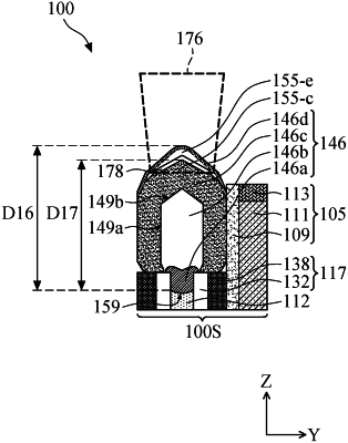
1. A semiconductor device structure, comprising:
a substrate having a plurality of fins formed from the substrate;
a first source/drain feature comprising:
a first epitaxial layer in contact with a first fin of the plurality of fins;
a second epitaxial layer formed on the first epitaxial layer; and
a third epitaxial layer formed on the second epitaxial layer, the third epitaxial layer comprising a center portion and an edge portion that is at a different height than the center portion; and
a fourth epitaxial layer formed on the third epitaxial layer; and
a second source/drain feature disposed adjacent to the first source/drain feature, the second source/drain feature comprising:
a first epitaxial layer in contact with a second fin of the plurality of fins;
a second epitaxial layer formed on the first epitaxial layer of the second source/drain feature;
a third epitaxial layer formed on the second epitaxial layer of the second source/drain feature, the third epitaxial layer comprising a center portion and an edge portion that is at a different height than the center portion of the third epitaxial layer of the second source/drain feature; and
a fourth epitaxial layer formed on the third epitaxial layer of the second source/drain feature,
wherein the center portion and the edge portion of the third epitaxial layer of the second source/drain feature are in contact with the center portion and edge portion of the third epitaxial layer of the first source/drain feature, respectively.
|