| CPC H01L 29/408 (2013.01) [H01L 21/0214 (2013.01); H01L 21/02164 (2013.01); H01L 21/0217 (2013.01); H01L 21/02178 (2013.01); H01L 21/28581 (2013.01); H01L 23/291 (2013.01); H01L 23/3171 (2013.01); H01L 29/2003 (2013.01); H01L 29/205 (2013.01); H01L 29/475 (2013.01); H01L 29/66462 (2013.01); H01L 29/7786 (2013.01); H01L 29/7787 (2013.01)] | 11 Claims |
|
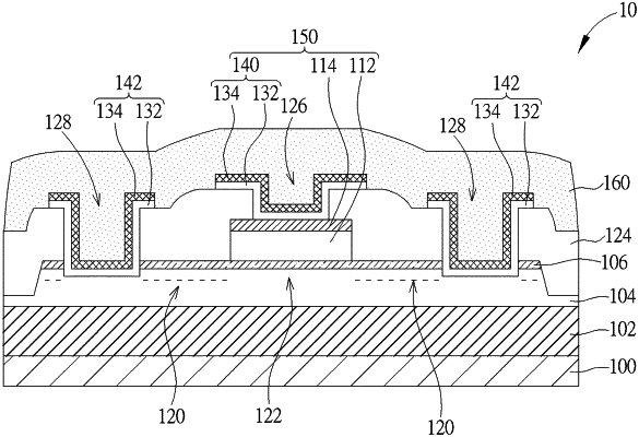
1. A method of fabricating a high electron mobility transistor, comprising:
providing a substrate having a group III-V channel layer, a group III-V barrier layer, a group III-V gate layer, and a gate etch stop layer disposed thereon;
forming a passivation layer covering the group III-V barrier layer and the gate etch stop layer;
forming a gate contact hole and at least one source/drain contact hole in the passivation layer, wherein the gate contact hole exposes the gate etch stop layer, and the at least one source/drain contact hole exposes the group III-V channel layer; and
forming a conductive layer conformally disposed on a top surface of the passivation layer and in the gate contact hole and the at least one source/drain contact hole.
|