| CPC H01L 29/404 (2013.01) [H01L 21/56 (2013.01); H01L 23/3171 (2013.01); H01L 23/3192 (2013.01); H01L 29/2003 (2013.01); H01L 29/401 (2013.01); H01L 29/41775 (2013.01); H01L 29/66462 (2013.01); H01L 29/7787 (2013.01)] | 20 Claims |
|
1. A semiconductor device, comprising:
a first nitride-based semiconductor layer disposed above a substrate;
a second nitride-based semiconductor layer disposed on the first nitride-based semiconductor layer and having a bandgap greater than a bandgap of the first nitride-based semiconductor layer;
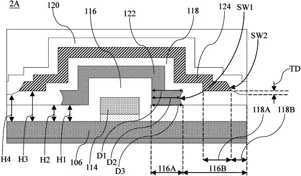
a gate electrode disposed above the second nitride-based semiconductor layer;
a first passivation layer disposed on the second nitride-based semiconductor layer and covering the gate electrode;
a first field plate disposed on the gate electrode and the first passivation layer, wherein the first passivation layer has a first portion covered with the first field plate and a second portion free from coverage of the first field plate;
a second passivation layer disposed on the first passivation layer and covering the first field plate; and
a second field plate disposed over the first field plate and the second passivation layer, wherein the second passivation layer has a first portion covered with the second field plate and a second portion is free from coverage of the second field plate, and a thickness difference between the first and second portions of the first passivation layer is less than a thickness difference between the first and second portions of the second passivation layer.
|