| CPC H01L 29/1037 (2013.01) [H01L 21/26586 (2013.01); H01L 29/0649 (2013.01); H01L 29/1083 (2013.01); H01L 29/66795 (2013.01); H01L 29/66803 (2013.01); H01L 29/7851 (2013.01)] | 20 Claims |
|
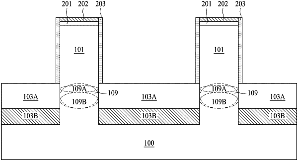
1. A FinFET structure, comprising:
a substrate;
a fin protruding from the substrate, comprising a first portion and a second portion below the first portion, wherein the first portion comprises a first dopant concentration of a dopant, and the second portion comprises a second dopant concentration of the dopant, the second dopant concentration is greater than the first dopant concentration;
a gate over the fin, wherein the second portion of the fin is below a bottom surface of the gate; and
an insulating layer over the substrate and proximal to the second portion of the fin, wherein at least a first portion of the insulating layer comprises a third dopant concentration of the dopant, the third dopant concentration is greater than the first dopant concentration.
|