| CPC H01L 29/086 (2013.01) [H01L 21/0465 (2013.01); H01L 29/063 (2013.01); H01L 29/1095 (2013.01); H01L 29/1608 (2013.01); H01L 29/32 (2013.01); H01L 29/66068 (2013.01); H01L 29/7813 (2013.01)] | 20 Claims |
|
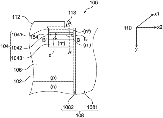
1. A semiconductor device, comprising:
a silicon carbide semiconductor body comprising a source region of a first conductivity type and a body region of a second conductivity type;
a trench structure extending from a first surface into the silicon carbide semiconductor body along a vertical direction, the trench structure comprising a gate electrode and a gate dielectric,
wherein the trench structure is stripe-shaped and runs along a longitudinal direction that is perpendicular to the vertical direction,
wherein the source region comprises a first source sub-region and a second source sub-region alternately arranged along the longitudinal direction,
wherein a doping concentration profile of the first source sub-region along the vertical direction differs from a doping concentration profile of the second source sub-region along the vertical direction.
|