| CPC H01L 28/60 (2013.01) [H10B 12/315 (2023.02)] | 20 Claims |
|
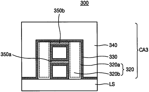
1. A semiconductor device comprising:
a substrate;
a lower electrode in a hole that extends in a vertical direction on the substrate;
a supporting layer that is on a side wall of the lower electrode and is configured to support the lower electrode;
a dielectric layer on the lower electrode and the supporting layer; and
an upper electrode on the dielectric layer,
wherein the lower electrode comprises an undoped region and a doped region,
wherein the doped region contacts the dielectric layer and the supporting layer,
wherein the undoped region is separated from the supporting layer by the doped region,
wherein the lower electrode comprises silicon or metal nitride, and
wherein the dielectric layer comprises hafnium oxide, zirconium oxide, aluminum oxide, or titanium oxide.
|