| CPC H01L 27/156 (2013.01) [G09G 3/32 (2013.01); H01L 33/382 (2013.01); H01L 33/62 (2013.01); G09G 2300/06 (2013.01); G09G 2320/0626 (2013.01)] | 20 Claims |
|
1. An electronic device comprising:
display driver circuitry;
an array of light-emitting diodes arranged in a light-emitting area;
an array of control circuits, wherein each one of the control circuits is configured to control at least one passive matrix of the light-emitting diodes based on signals from the display driver circuitry; and
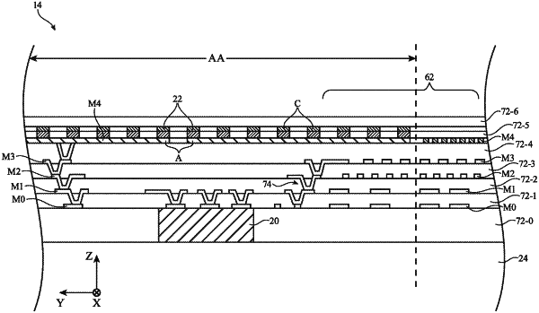
fanout signal lines that are coupled to the display driver circuitry and that receive the signals from the display driver circuitry, wherein the fanout signal lines at least partially overlap the light-emitting area and wherein the fanout signal lines include a first patterned metal layer, a second patterned metal layer that is formed over the first patterned metal layer, a third patterned metal layer that is formed over the second patterned metal layer, a fourth patterned metal layer that is formed over the third patterned metal layer, and a fifth patterned metal layer that is formed over the fourth patterned metal layer.
|