| CPC H01L 27/156 (2013.01) [G09F 9/33 (2013.01); H01L 33/56 (2013.01); H01L 33/62 (2013.01)] | 20 Claims |
|
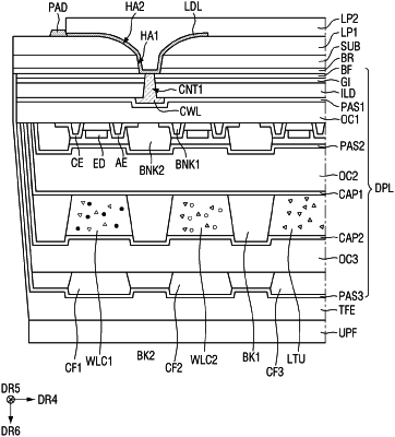
1. A display device, comprising:
a display layer including pixels each including at least one transistor;
a connection wiring electrically connected to the at least one transistor and exposed to a lower surface of the display layer through a first contact hole in the display layer;
a base member disposed under the display layer and including a first hole exposing the connection wiring exposed to the lower surface of the display layer;
a first lower protective layer disposed on a lower surface of the base member and including a second hole overlapping the first hole in a thickness direction of the base member;
a pad portion disposed on a lower surface of the first lower protective layer; and
a lead line disposed on the lower surface of the first lower protective layer and electrically connecting the pad portion and the connection wiring.
|