| CPC H01L 27/14689 (2013.01) [H01L 27/14621 (2013.01); H01L 27/14627 (2013.01); H01L 27/14643 (2013.01)] | 20 Claims |
|
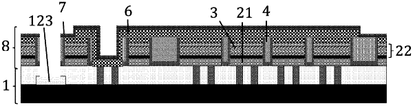
1. A method for forming a pixelated optoelectronic stack on a substrate, the method comprising:
forming a stacked layer structure on a substrate, the stacked layer structure comprising:
a bottom electrode layer;
an optoelectronic layer over the bottom electrode layer; and
a patterned hard-mask over the optoelectronic layer, wherein a pattern of the patterned hard-mask comprises at least two hard-mask islands separated by a hard-mask-free area;
replicating the pattern into the optoelectronic layer and the bottom electrode layer by etching through the optoelectronic layer and the bottom electrode layer selectively with respect to the hard-mask, thereby forming a first intermediate pixelated stack on top of the substrate, the first intermediate pixelated stack comprising at least two islands of stack separated from one another by stack-free areas;
forming an electrically insulating layer on the first intermediate pixelated stack to fill the stack-free areas and cover the at least two islands of stack;
removing a top portion of the electrically insulating layer and removing any remaining hard-mask so that a top surface of the electrically insulating layer is coplanar with an exposed top surface of the first intermediate pixelated stack, yielding a second intermediate pixelated stack on top of the substrate; and
forming a top transparent electrode layer over the second intermediate pixelated stack.
|