| CPC H01L 27/14612 (2013.01) [H01L 27/14636 (2013.01); H01L 27/14638 (2013.01); H01L 27/14641 (2013.01); H01L 27/14643 (2013.01); H01L 27/14683 (2013.01)] | 19 Claims |
|
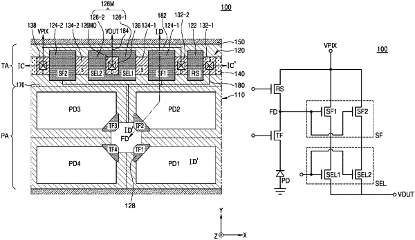
1. An image sensor, comprising:
a pixel area, the pixel area including
a photodiode, and
a floating diffusion area; and
a transistor area adjacent to the pixel area in a first direction, the transistor area including
a plurality of transistors disposed along a second direction perpendicular to the first direction, the plurality of transistors including
a first source follower transistor,
a second source follower transistor, and
a plurality of selection transistors,
wherein gates of the first source follower transistor and the second source follower transistor are connected to the floating diffusion area, and
wherein the first source follower transistor and the second source follower transistor are substantially symmetrical to each other about a center between the first source follower transistor and the second source follower transistor in the second direction, such that
the transistor area includes a first portion and a second portion, the first portion extending from the center to the first source follower transistor in the second direction, the second portion extending from the center to the second source follower transistor in the second direction, and the first and second portions of the transistor area have reflective symmetry to each other about the center in the second direction.
|