| CPC H01L 27/1244 (2013.01) [G02F 1/133345 (2013.01); G02F 1/134309 (2013.01); G02F 1/136286 (2013.01); G02F 1/1368 (2013.01)] | 17 Claims |
|
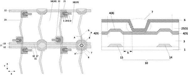
1. An array substrate, comprising:
a plurality of gate lines;
a plurality of data lines intersecting with the plurality of gate lines;
a plurality of pixel units, wherein the plurality of gate lines and the plurality of data lines are arranged between at least part of adjacent pixel units;
a plurality of common electrode lead wires; and
a common electrode layer arranged on the plurality of common electrode lead wires;
wherein the plurality of common electrode lead wires are arranged on a same layer as the plurality of data lines, extend in a same direction as the plurality of data lines, and are located between at least part of adjacent pixel units;
the common electrode layer is insulated from the plurality of common electrode lead wires through an insulating layer and is connected to the plurality of common electrode lead wires through via holes in the insulating layer, wherein the via holes are located in regions where the plurality of gate lines and the plurality of common electrode lead wires intersect; and
the plurality of gate lines each comprise a linear portion extending in a first direction away from the via holes, and comprise a curved portion curvedly surrounding edges of the via holes close to the via holes, wherein the curved portion is an avoidance portion for avoiding the via holes.
|
|
9. A display panel, comprising: an array substrate, an opposite substrate arranged opposite to the array substrate, and a liquid crystal layer arranged between the array substrate and the opposite substrate; wherein the array substrate comprises:
a plurality of gate lines;
a plurality of data lines intersecting with the plurality of gate lines;
a plurality of pixel units, wherein the plurality of gate lines and the plurality of data lines are arranged between at least part of adjacent pixel units;
a plurality of common electrode lead wires; and
a common electrode layer arranged on the plurality of common electrode lead wires;
wherein the plurality of common electrode lead wires are arranged on a same layer as the plurality of data lines, extend in a same direction as the plurality of data lines, and are located between at least part of adjacent pixel units;
the common electrode layer is insulated from the plurality of common electrode lead wires through an insulating layer and is connected to the plurality of common electrode lead wires through via holes in the insulating layer, wherein the via holes are located in regions where the plurality of gate lines and the plurality of common electrode lead wires intersect; and
the plurality of gate lines each comprise a linear portion extending in a first direction away from the via holes, and comprise a curved portion curvedly surrounding edges of the via holes close to the via holes, wherein the curved portion is an avoidance portion for avoiding the via holes.
|
|
17. A display apparatus, comprising: a display panel comprising an array substrate, an opposite substrate arranged opposite to the array substrate, and a liquid crystal layer arranged between the array substrate and the opposite substrate; wherein the array substrate comprises:
a plurality of gate lines;
a plurality of data lines intersecting with the plurality of gate lines;
a plurality of pixel units, wherein the plurality of gate lines and the plurality of data lines are arranged between at least part of adjacent pixel units;
a plurality of common electrode lead wires; and
a common electrode layer arranged on the plurality of common electrode lead wires;
wherein the plurality of common electrode lead wires are arranged on a same layer as the plurality of data lines, extend in a same direction as the plurality of data lines, and are located between at least part of adjacent pixel units;
the common electrode layer is insulated from the plurality of common electrode lead wires through an insulating layer and is connected to the plurality of common electrode lead wires through via holes in the insulating layer, wherein the via holes are located in regions where the plurality of gate lines and the plurality of common electrode lead wires intersect; and
the plurality of gate lines each comprise a linear portion extending in a first direction away from the via holes, and comprise a curved portion curvedly surrounding edges of the via holes close to the via holes, wherein the curved portion is an avoidance portion for avoiding the via holes.
|