| CPC H01L 27/1244 (2013.01) [G02F 1/136286 (2013.01); H01L 27/1255 (2013.01); G02F 1/13606 (2021.01); G02F 1/136227 (2013.01); G02F 1/1368 (2013.01)] | 16 Claims |
|
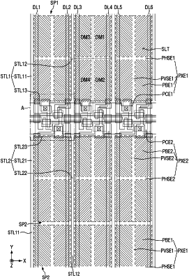
1. A display device comprising:
a substrate;
scan lines disposed on the substrate and extending along a first direction;
data lines disposed on the substrate and extending along a second direction that intersects the first direction;
a first switching element including a first active area, a first gate electrode connected to a first scan line among the scan lines, a first drain electrode connected to a first data line among the data lines, and a first source electrode facing the first drain electrode;
a first pixel electrode disposed on a first side of the first scan line and connected to the first source electrode of the first switching element;
a second switching element including a second active area, a second gate electrode connected to the first scan line, a second drain electrode connected to a second data line among the data lines, and a second source electrode facing the second drain electrode; and
a second pixel electrode disposed on a second side of the first scan line and connected to the second source electrode of the second switching element,
a first source connector which extends from the first source electrode and is connected to the first pixel electrode through a first contact hole; and
a second source connector which extends from the second source electrode and is connected to the second pixel electrode through a second contact hole,
wherein the first pixel electrode and the second pixel electrode are disposed along the second direction with the first switching element and the second switching element disposed between the first pixel electrode and the second pixel electrode,
wherein the first contact hole overlaps the second transistor in the first direction, and
wherein the second contact hole overlaps the first transistor in the first direction.
|