| CPC H01L 27/1237 (2013.01) [H01L 27/1259 (2013.01)] | 19 Claims |
|
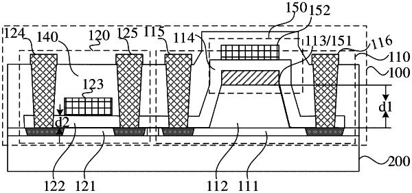
1. An array substrate, comprising:
a thin film transistor array layer, wherein the thin film transistor array layer comprises a driving transistor, a switching transistor and a capacitor,
wherein the driving transistor comprises a first active layer, a first gate insulating layer, a first gate and an insulating dielectric layer sequentially stacked;
the switching transistor comprises a second active layer, a second gate insulating layer and a second gate sequentially stacked; and
the insulating dielectric layer and the second gate insulating layer are located at a same layer; a thickness of the first gate insulating layer is greater than a thickness of the second gate insulating layer; the capacitor comprises a first electrode plate and a second electrode plate, wherein the first electrode plate and the first gate are disposed in a same layer, and the second electrode plate and the second gate are disposed in a same layer.
|