| CPC H01L 27/0886 (2013.01) [H01L 21/3212 (2013.01); H01L 21/76802 (2013.01); H01L 21/7684 (2013.01); H01L 21/76843 (2013.01); H01L 21/7685 (2013.01); H01L 21/823475 (2013.01); H01L 23/5283 (2013.01); H01L 23/53238 (2013.01); H01L 23/53252 (2013.01); H01L 23/53266 (2013.01); H01L 23/535 (2013.01); H01L 29/0673 (2013.01)] | 19 Claims |
|
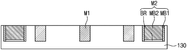
1. A semiconductor device, comprising:
an interlayer dielectric layer on a substrate;
a first connection line that fills a first trench of the interlayer dielectric layer, the first trench having a first width; and
a second connection line that fills a second trench of the interlayer dielectric layer, the second trench having a second width greater than the first width, and the second connection line including:
a first metal layer that covers an inner sidewall of the second trench,
a barrier layer that covers a bottom surface of the second trench, and
a second metal layer on the first metal layer and the barrier layer,
wherein both the first metal layer and the barrier layer are in direct contact with the interlayer dielectric layer,
wherein the first connection line and the first metal layer include a first metal, and
wherein the second metal layer includes a second metal different from the first metal.
|