| CPC H01L 27/0262 (2013.01) [H01L 27/0207 (2013.01); H01L 27/0255 (2013.01); H01L 29/87 (2013.01); H01L 23/60 (2013.01); H01L 23/62 (2013.01); H01L 27/0248 (2013.01); H01L 27/0652 (2013.01); H01L 27/0658 (2013.01); H01L 29/0804 (2013.01); H01L 29/0821 (2013.01); H01L 29/1004 (2013.01); H01L 29/747 (2013.01); H01L 29/8611 (2013.01); H01L 2924/13034 (2013.01); H01L 2924/13035 (2013.01)] | 20 Claims |
|
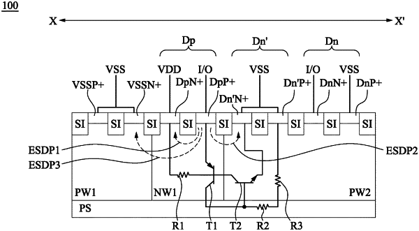
1. A semiconductor device, comprising:
first and second doped regions that are disposed in a first well on a substrate, included in a structure operating as a first diode, and coupled to a first voltage terminal;
a third doped region that is in a second well and coupled to an input/output (I/O) pad,
wherein the first doped region and the second well have the same conductivity type, and the third doped region and the first well have the same conductivity type,
wherein the first doped region and the third doped region are configured to transmit a first electrostatic discharge (ESD) current flowing between the I/O pad and the first voltage terminal providing a first supply voltage; and
a fourth doped region that is disposed in a third well, different from the first and second wells, and coupled to the first and second doped regions, wherein the third and fourth doped regions are configured as a current discharge path.
|