|
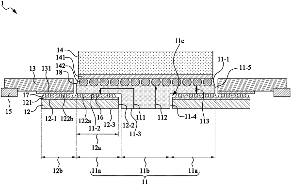
1. An optoelectronic package structure, comprising: a carrier comprising a first region and a second region adjacent to the first region; an electronic component disposed under the first region of the carrier; a photonic component disposed over the electronic component; a first power supply path in the carrier, wherein the first power supply path electrically connects the electronic component; a processing unit disposed over the second region, wherein the processing unit covers the second region from a top view perspective; and a second power supply path in the carrier and electrically connects the processing unit; wherein the processing unit is disposed adjacent to a first surface of the carrier, and the electronic component is disposed adjacent to a second surface of the carrier opposite to the first surface.
|