| CPC H01L 25/0753 (2013.01) [H01L 33/382 (2013.01); H01L 33/54 (2013.01); H01L 33/58 (2013.01); H01L 33/62 (2013.01)] | 12 Claims |
|
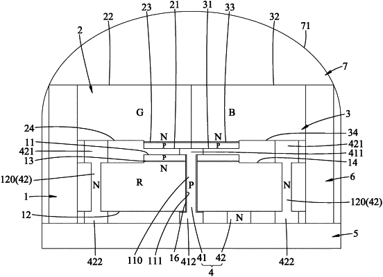
1. A mixed light light-emitting diode device, comprising:
a first chip including
a first chip first-type semiconductor layer having a first chip first surface,
a first chip P-N junction layer,
a first chip second-type semiconductor layer stacked with said first chip first-type semiconductor layer and said first chip P-N junction layer, and having a first chip second surface opposite to said first chip first surface and a first chip third surface indenting from said first chip first surface and situated on said first chip second-type semiconductor layer,
a first through hole penetrating through said first chip first surface, said first chip P-N junction layer, and said first chip second surface, and
two second through holes, each of which penetrates through said first chip second and third surfaces, and is spaced apart from said first through hole;
a second chip spacedly disposed above said first chip, and including
a second chip first-type semiconductor layer having a second chip first surface which faces said first chip first surface, and
a second chip second-type semiconductor layer having a second chip second surface opposite to said second chip first surface;
a third chip spacedly disposed above said first chip, and including
a third chip first-type semiconductor layer having a third chip first surface which faces said first chip first surface, and
a third chip second-type semiconductor layer having a third chip second surface opposite to said third chip first surface; and
an electrode unit including
a first-type electrode disposed in said first through hole in an electrically isolated manner, and connecting all of said first chip, second chip and third chip first-type semiconductor layers, and
three second-type electrodes, two of said second-type electrodes being respectively disposed in said second through holes, each of said two of said second-type electrodes connecting one of said second chip and third chip second-type semiconductor layers to said first chip second-type semiconductor layer, a remaining one of said second-type electrodes being disposed on said first chip second surface and between said first-type electrode and one of said two of said second-type electrodes.
|