| CPC H01L 25/0657 (2013.01) [H01L 21/78 (2013.01); H01L 23/562 (2013.01); H01L 25/50 (2013.01); H01L 2225/06513 (2013.01); H01L 2225/06541 (2013.01); H01L 2225/06548 (2013.01); H01L 2225/06586 (2013.01)] | 20 Claims |
|
1. A method for packaging a semiconductor, comprising:
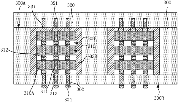
providing a substrate wafer, the substrate wafer having a first surface and a second surface arranged opposite to each other, the first surface having a plurality of grooves, wherein a plurality of electrically conductive pillars are provided at a bottom of a given one of the plurality of grooves, and the plurality of electrically conductive pillars penetrate through the bottom of the given groove to the second surface of the substrate wafer;
providing a plurality of semiconductor die stacks in the plurality of grooves such that a given one of the plurality of semiconductor die stacks is provided in a corresponding one of the plurality of grooves, wherein an upper surface of the given semiconductor die stack is lower than or flush with an upper edge of the corresponding groove, and a bottom of the given semiconductor die stack is electrically connected to the plurality of electrically conductive pillars provided at the bottom of the corresponding groove; and
filling an insulating dielectric in gaps among sidewalls of the plurality of grooves and the plurality of semiconductor die stacks to form an insulating dielectric layer, the insulating dielectric layer covering upper surface of the plurality of semiconductor die stacks to seal up the plurality of semiconductor die stacks to form a semiconductor package structure.
|