| CPC H01L 24/20 (2013.01) [H01L 24/19 (2013.01); H01L 21/568 (2013.01); H01L 24/13 (2013.01); H01L 2224/13024 (2013.01); H01L 2224/19 (2013.01); H01L 2224/221 (2013.01)] | 20 Claims |
|
1. A structure comprising:
a device die;
an encapsulant encapsulating the device die therein;
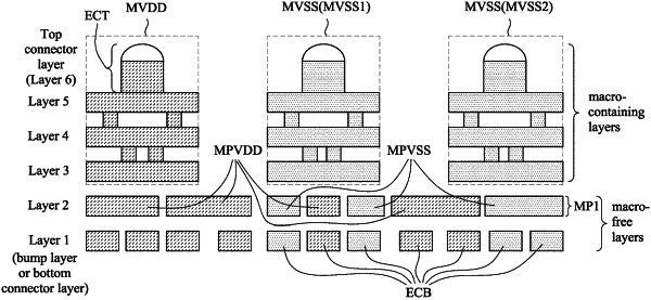
a redistribution structure over and electrically connected to the device die, wherein the redistribution structure comprises a bottom layer and a plurality of upper layers over the bottom layer, and wherein the redistribution structure comprises:
a first power-ground macro extending from a topmost layer in the plurality of upper layers to a bottommost layer in the plurality of upper layers;
a second power-ground macro extending from the topmost layer in the plurality of upper layers to the bottommost layer in the plurality of upper layers;
at least one first conductive feature in the bottom layer and overlapped by the first power-ground macro; and
at least one second conductive feature in the bottom layer and overlapped by the second power-ground macro, wherein patterns of the at least one first conductive feature are different from the at least one second conductive feature.
|