| CPC H01L 24/09 (2013.01) [H01L 21/52 (2013.01); H01L 21/568 (2013.01); H01L 23/5386 (2013.01); H01L 23/5389 (2013.01); H01L 24/17 (2013.01); H01L 24/19 (2013.01); H01L 24/20 (2013.01); H01L 24/81 (2013.01); H01L 25/0652 (2013.01); H01L 23/3128 (2013.01); H01L 23/49816 (2013.01); H01L 25/105 (2013.01); H01L 2224/02331 (2013.01); H01L 2224/0401 (2013.01); H01L 2224/04105 (2013.01); H01L 2224/12105 (2013.01); H01L 2224/16235 (2013.01); H01L 2224/27002 (2013.01); H01L 2224/32245 (2013.01); H01L 2224/73267 (2013.01); H01L 2224/83191 (2013.01); H01L 2224/92244 (2013.01); H01L 2224/96 (2013.01); H01L 2225/1035 (2013.01); H01L 2225/1041 (2013.01); H01L 2225/1058 (2013.01); H01L 2924/351 (2013.01)] | 20 Claims |
|
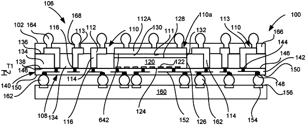
1. A microelectronic assembly comprising:
a microelectronic element having a front surface, an opposed rear surface, and bond pads disposed at the front surface;
a redistribution structure configured to conductively connect bond pads of the microelectronic element with terminals of the microelectronic assembly;
a plurality of back side conductive components, the plurality of back side conductive components being etched monolithic structures, the plurality of back side conductive components further comprising a back side routing layer and an interconnection element integrally formed with the back side routing layer and extending in a direction away from the back side routing layer, and wherein the back side routing layer of at least one of the plurality of back side conductive components overlies the rear surface of the microelectronic element; and
an encapsulant comprising opposed interconnection surfaces, and disposed between each interconnection element of the plurality of back side conductive components, wherein the back side routing layer of the at least one of the plurality of back side conductive components extends along one of the opposed interconnection surfaces.
|