| CPC H01L 24/08 (2013.01) [H01L 24/05 (2013.01); H01L 24/80 (2013.01); H01L 2224/05016 (2013.01); H01L 2224/05147 (2013.01); H01L 2224/08145 (2013.01); H01L 2224/80895 (2013.01); H01L 2224/80896 (2013.01); H01L 2924/01029 (2013.01); H01L 2924/05042 (2013.01); H01L 2924/05442 (2013.01); H01L 2924/351 (2013.01)] | 19 Claims |
|
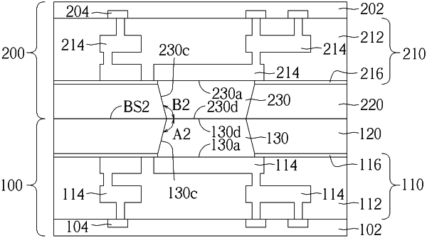
1. A semiconductor structure for wafer level bonding, comprising:
an interconnecting layer comprising a plurality of interconnecting structures disposed on a substrate,
an etching stop layer on the interconnecting layer and directly contacting top surfaces of the interconnecting structures;
a bonding dielectric layer disposed on a the etching stop layer; and
a bonding pad disposed in the bonding dielectric layer and through the etching stop layer to directly contact one of the interconnecting structures, wherein the bonding pad comprises:
a top surface exposed from the bonding dielectric layer;
a bottom surface opposite to the top surface; and
a sidewall between the top surface and the bottom surface, wherein a bottom angle between the sidewall and the bottom surface of the bonding pad is smaller than 90 degrees.
|