| CPC H01L 24/06 (2013.01) [B23K 1/0056 (2013.01); H01L 24/03 (2013.01); H05K 3/34 (2013.01); H01L 2224/0363 (2013.01); H05K 2203/107 (2013.01)] | 22 Claims |
|
5. A method of making a semiconductor device, comprising:
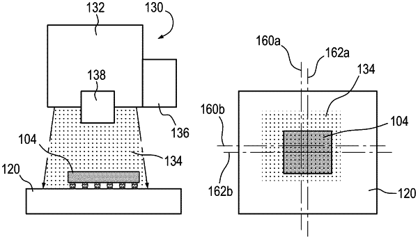
disposing a semiconductor die over a substrate;
disposing a beam homogenizer over the semiconductor die using a first camera, wherein a beam from the beam homogenizer impacts the semiconductor die;
calculating a positional offset of the beam relative to the semiconductor die in a first unit using image processing on an image from a second camera, wherein the second camera is a different type of camera from the first camera;
using a first calibration equation to convert the positional offset into a first distance in a second unit;
moving the beam homogenizer the first distance to center the semiconductor die fully within the beam;
calculating a rotational offset of the beam relative to the semiconductor die in a third unit;
using a second calibration equation to convert the rotational offset into a second distance in a fourth unit; and
rotating the beam homogenizer the second distance to rotationally align the beam to the semiconductor die.
|