| CPC H01L 23/53295 (2013.01) [H01L 21/76802 (2013.01); H01L 21/76832 (2013.01); H01L 21/76835 (2013.01); H01L 21/76807 (2013.01); H01L 21/7684 (2013.01)] | 20 Claims |
|
1. A method of forming a semiconductor device, comprising:
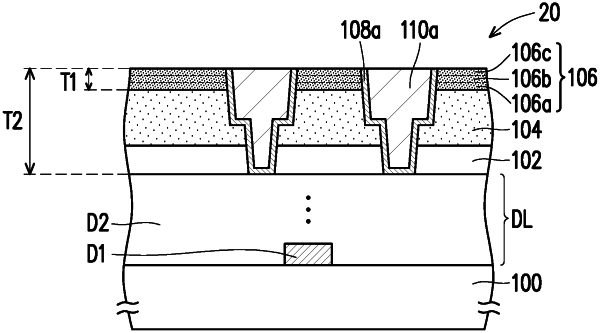
forming an etch stop layer over the substrate, wherein the etch stop layer is a four-layer structure comprising, from bottom to top, AlOxNy, SiCO, AlOx and SiCO;
forming a low-k dielectric layer over etch stop layer;
forming a cap layer on the low-k dielectric layer, wherein a carbon atom content of the cap layer ranges from 20 at % to 35 at % and is greater than a carbon atom content of the low-k dielectric layer;
forming a patterned hard mask layer on the cap layer;
patterning the cap layer and the low-k dielectric layer by using the patterned hard mask layer as a mask, thereby forming an opening in the cap layer and the low-k dielectric layer; and
forming a conductive layer in the opening.
|