| CPC H01L 23/53257 (2013.01) [H01L 21/76805 (2013.01); H01L 21/76883 (2013.01); H01L 21/76888 (2013.01); H01L 23/5226 (2013.01)] | 20 Claims |

|
1. A method, comprising:
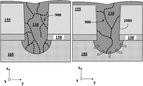
depositing an etch stop layer on a cobalt contact disposed on a substrate;
depositing a dielectric layer on the etch stop layer;
etching the dielectric layer and the etch stop layer to form an opening to expose a top surface of the cobalt contact;
etching the exposed top surface of the cobalt contact to form a recess in the cobalt contact, wherein the recess extends laterally under the etch stop layer;
depositing a ruthenium metal to substantially fill the recess and the opening; and
annealing the ruthenium metal to convert a portion of the ruthenium metal that is in physical contact with the dielectric layer into a conductive ruthenium oxide layer along interfaces between the ruthenium metal and the dielectric layer and to limit cobalt concentration to less than about 6 atomic percent along grain boundaries in the ruthenium metal.
|