| CPC H01L 23/53238 (2013.01) [H01L 21/324 (2013.01); H01L 21/76876 (2013.01); H01L 23/5226 (2013.01)] | 20 Claims |
|
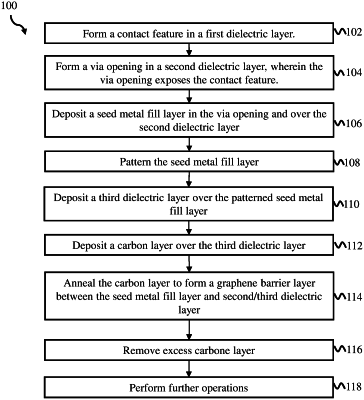
1. A method, comprising:
forming a first contact feature in a first dielectric layer over a workpiece;
forming a second dielectric layer over the first contact feature and the first dielectric layer;
forming a via opening in the second dielectric layer to expose a portion of the first contact feature;
depositing a seed metal layer in the via opening and over the second dielectric layer;
patterning the seed metal layer to expose a portion of the second dielectric layer;
depositing a third dielectric layer over the exposed portion of the second dielectric layer;
depositing a carbon layer over the seed metal layer and the third dielectric layer; and
annealing the workpiece to form a graphene layer between the seed metal layer and the third dielectric layer.
|