| CPC H01L 23/5226 (2013.01) [H01L 21/28562 (2013.01); H01L 21/76816 (2013.01); H01L 21/76843 (2013.01); H01L 21/76852 (2013.01); H01L 21/76879 (2013.01); H01L 21/823431 (2013.01); H01L 21/823475 (2013.01); H01L 23/5283 (2013.01); H01L 27/0886 (2013.01); H01L 29/41791 (2013.01); H01L 29/66795 (2013.01); H01L 29/785 (2013.01)] | 20 Claims |
|
1. A method for forming a semiconductor device structure, comprising:
forming a first insulating layer over a substrate;
forming a first metal feature in the first insulating layer;
forming a second insulating layer over the first insulating layer;
forming a first metal via through the second insulating layer to connect the first metal feature; and
forming a second metal feature over the second insulating layer, wherein the second metal feature has a convex top surface and wherein an interface between the second metal feature and the second insulating layer is substantially and horizontally aligned to an interface between the second metal feature and the first metal via.
|
|
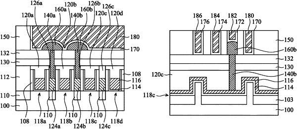
9. A method for forming a semiconductor device structure, comprising:
forming a first gate electrode layer and a first source/drain contact over a substrate;
forming a first metal via to connect the first gate electrode layer, and a second metal via to connect the first source/drain contact;
forming an organic film including amphiphilic-like molecules as a metal inhibition layer over the first gate electrode layer and the first source/drain contact, wherein the organic film exposes a top surface of the first metal via and a top surface of the second metal via; and
growing a first metal feature with a convex top surface from the exposed top surface of the first metal via and a second metal feature with a convex top surface from the exposed top surface of the second metal via by a deposition process using the metal inhibition layer.
|
|
15. A method for forming a semiconductor device structure, comprising:
forming a first insulating layer over a substrate having a fin structure;
forming a first gate electrode layer in the first insulating layer and across the fin structure;
forming a first source/drain contact electrically connected to a first source/drain region in the fin structure;
forming a second insulating layer over the first insulating layer;
etching the second insulating layer to form a first via opening exposing the first gate electrode layer and a second via opening exposing the first source/drain contact;
forming a first metal via in the first via opening to connect the first gate electrode layer, and a second metal via in the second via opening to connect the first source/drain contact;
forming a third insulating layer over the second insulating layer;
etching the third insulating layer to form a first trench opening exposing the first metal via and a second trench opening exposing the second metal via; and
selectively growing a first metal hump from a top surface of the first metal via and a second metal hump from a top surface of the second metal via.
|