| CPC H01L 23/3121 (2013.01) [H01L 23/5283 (2013.01); H01L 23/5389 (2013.01); H01L 24/10 (2013.01); H01L 24/82 (2013.01); H01L 2924/01029 (2013.01); H01L 2924/1811 (2013.01)] | 14 Claims |
|
1. A method of forming an integrated circuit (IC) package, the method comprising:
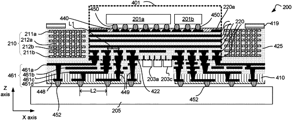
forming a substrate comprising a sacrificial material, wherein the forming comprises:
forming a first interconnect layer having a first pitch and embedded within the substrate, adjacent to the sacrificial material; and
forming a second interconnect layer with a second pitch, smaller than the first pitch, over a first side of the sacrificial material and over the first interconnect layer;
removing the sacrificial material to form a recess within the substrate, the recess exposing at least a part of the second interconnect layer, wherein removing the sacrificial material comprises exposing the sacrificial material by removing a first portion of the substrate exposed by the forming of the first interconnect layer; and
attaching one or more components within the recess, and to the second interconnect layer.
|