| CPC H01L 21/823807 (2013.01) [H01L 21/823814 (2013.01); H01L 21/823821 (2013.01); H01L 21/823878 (2013.01); H01L 27/0924 (2013.01)] | 20 Claims |

|
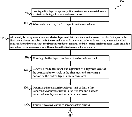
1. A device comprising:
first semiconductor layers disposed over a first area of a substrate, wherein the first semiconductor layers are separated from each other and are stacked up along a direction generally perpendicular to a top surface of the substrate, wherein one of the first semiconductor layers has a top surface facing away from the substrate and positioned at a first height above the substrate;
second semiconductor layers disposed over a second area of the substrate, wherein the second semiconductor layers are separated from each other and are stacked up along the direction generally perpendicular to the top surface of the substrate, wherein the first semiconductor layers include a first semiconductor material, and the second semiconductor layers include a second semiconductor material different from the first semiconductor material, wherein one of the second semiconductor layers has a top surface facing away from the substrate and positioned at the first height above the substrate;
a first gate structure wrapping around each of the first semiconductor layers; and
a second gate structure wrapping around each of the second semiconductor layers.
|