| CPC H01L 21/823468 (2013.01) [H01L 29/42392 (2013.01); H01L 29/78696 (2013.01)] | 20 Claims |
|
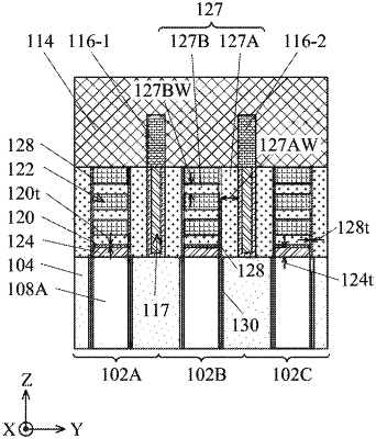
1. A semiconductor structure, comprising:
a substrate;
a fin bottom portion on the substrate;
a stacked nanostructure comprising a plurality of layers on the fin bottom portion; and
an isolation layer between the stacked nanostructure and the fin bottom portion;
a dielectric liner on a sidewall of the stacked nanostructure and in contact with an end of the stacked nanostructure; and
a spacer structure between the plurality of layers of the stacked nanostructure and in contact with the dielectric liner.
|