| CPC H01L 21/76832 (2013.01) [H01L 21/76816 (2013.01); H01L 21/76885 (2013.01); H01L 23/5283 (2013.01); H10B 12/482 (2023.02)] | 15 Claims |
|
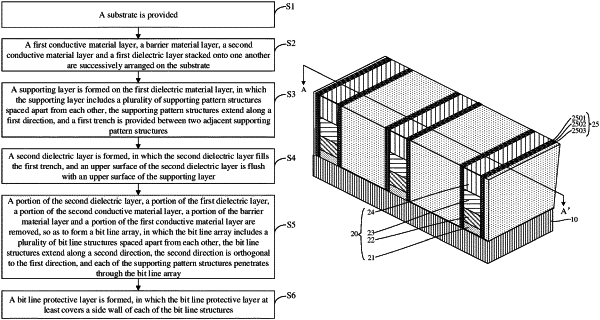
1. A method for preparing a semiconductor structure, comprising:
providing a substrate;
successively arranging a first conductive material layer, a barrier material layer, a second conductive material layer and a first dielectric material layer on the substrate stacked onto one another;
forming a supporting layer on the first dielectric material layer, the supporting layer comprising a plurality of supporting pattern structures spaced apart from each other, the supporting pattern structures extending along a first direction, and a first trench being provided between two adjacent supporting pattern structures;
forming a second dielectric layer, the second dielectric layer filling the first trench, and an upper surface of the second dielectric layer being flush with an upper surface of the supporting layer;
removing a portion of the second dielectric layer, a portion of the first dielectric material layer, a portion of the second conductive material layer, a portion of the barrier material layer and a portion of the first conductive material layer to form a bit line array, wherein the bit line array comprises a plurality of bit line structures spaced apart from each other, the bit line structures extend along a second direction, the second direction is orthogonal to the first direction, and each of the supporting pattern structures penetrates through the bit line array; and
forming a bit line protective layer, the bit line protective layer at least covering a side wall of each of the bit line structures.
|