| CPC H01L 21/7682 (2013.01) [H01L 21/76805 (2013.01); H01L 21/76846 (2013.01); H01L 21/76849 (2013.01); H01L 21/76895 (2013.01); H01L 23/5329 (2013.01); H01L 23/535 (2013.01)] | 20 Claims |
|
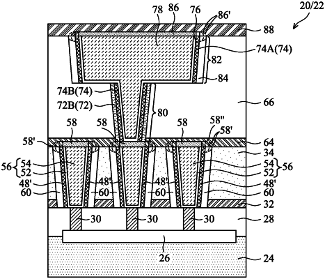
1. A method comprising:
etching a dielectric layer to form an opening, wherein a first conductive feature underlying the dielectric layer is exposed to the opening;
depositing a sacrificial spacer layer extending into the opening;
performing a first etching process to etch the sacrificial spacer layer, wherein a first bottom portion of the sacrificial spacer layer at a bottom of the opening is removed to reveal the first conductive feature, and a first vertical portion of the sacrificial spacer layer in the opening and on a sidewall of the dielectric layer is left to form a sacrificial ring;
depositing a protection layer extending into the opening and on the sacrificial ring;
performing a second etching process to etch the protection layer, wherein a second bottom portion of the protection layer is removed to reveal the first conductive feature, and a second vertical portion of the protection layer in the opening is left to form a protection ring;
forming a second conductive feature in the opening, wherein the second conductive feature is encircled by the sacrificial ring, and is over and electrically coupled to the first conductive feature; and
removing the sacrificial ring to form an air spacer.
|
|
13. A method comprising:
forming a first etch stop layer over a first conductive feature;
forming a dielectric layer over the first etch stop layer;
forming a structure comprising:
a second conductive feature in the dielectric layer and the first etch stop layer, wherein the second conductive feature is over and electrically coupling to the first conductive feature;
a protection ring encircling the second conductive feature; and
a sacrificial ring encircling the protection ring; and
removing the sacrificial ring to form an air spacer encircling the protection ring, wherein sidewalls of the dielectric layer are exposed to the air spacer.
|
|
18. A method comprising:
forming a first dielectric layer;
forming a first conductive feature in the first dielectric layer;
forming a second conductive feature over and electrically coupling to the first conductive feature, wherein the second conductive feature comprises:
a diffusion barrier; and
a metallic material encircled by the diffusion barrier;
forming a protection ring encircling and contacting the second conductive feature, wherein the protection ring contacts a top surface of at least one of the first dielectric layer and the first conductive feature; and
forming an air spacer encircling the protection ring, wherein the air spacer separates the protection ring from a second dielectric layer that encircles the air spacer.
|