| CPC H01L 21/67373 (2013.01) [H01L 21/67303 (2013.01); H01L 21/67706 (2013.01); H01L 21/6773 (2013.01); H01L 21/67736 (2013.01)] | 20 Claims |
|
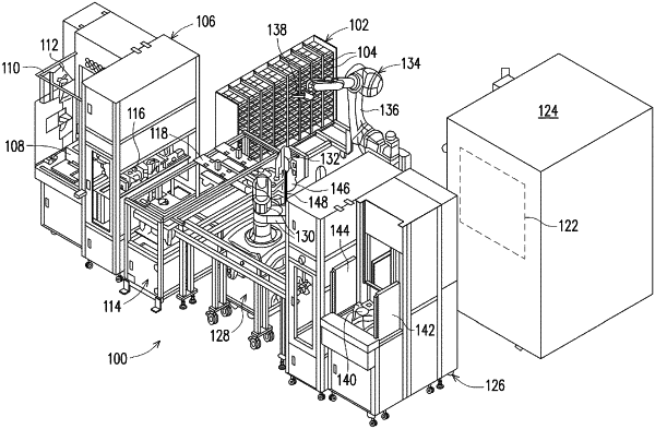
1. A system for manufacturing a semiconductor electronic device, comprising:
an assembler configured to receive a jig and a boat supporting a die, wherein the assembler comprises:
a separator configured to separate the jig into a first jig portion and a second jig portion, and
a loader configured to position the boat adjacent to the first jig portion, wherein the separator is configured to position the second jig portion adjacent to the boat to form an assembly comprising the boat arranged between the first jig portion and the second jig portion;
a robot configured to receive the assembly prepared by the assembler and manipulate a locking system that fixes an alignment of the boat relative to the first jig portion and the second jig portion to form a locked assembly; and
a process chamber configured to receive the locked assembly and subject the locked assembly to a fabrication operation.
|