US 11,929,271 B2
Apparatus and method for inspecting wafer carriers
Cheng-Kang Hu, Kaohsiung (TW); Shou-Wen Kuo, Hsinchu (TW); Sheng-Hsiang Chuang, Hsin-Chu (TW); Jiun-Rong Pai, Jhubei (TW); and Hsu-Shui Liu, Pingjhen (TW)
Assigned to Taiwan Semiconductor Manufacturing Co., Ltd., Hsin-Chu (TW)
Filed by Taiwan Semiconductor Manufacturing Co., Ltd., Hsin-Chu (TW)
Filed on Jul. 13, 2020, as Appl. No. 16/927,089.
Application 16/927,089 is a continuation of application No. 15/965,701, filed on Apr. 27, 2018, granted, now 10,714,364.
Claims priority of provisional application 62/552,972, filed on Aug. 31, 2017.
Prior Publication US 2020/0343115 A1, Oct. 29, 2020
This patent is subject to a terminal disclaimer.
Int. Cl. H01L 21/67 (2006.01); G01M 3/38 (2006.01); H01L 21/677 (2006.01)
CPC H01L 21/67265 (2013.01) [G01M 3/38 (2013.01); H01L 21/67259 (2013.01); H01L 21/67288 (2013.01); H01L 21/67772 (2013.01)] 20 Claims
OG exemplary drawing
 
1. An apparatus for inspecting wafer carriers, comprising:
a housing;
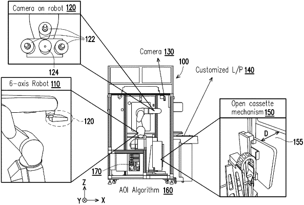
a load port configured to load a wafer carrier into the housing;
a robot arm inside the housing, wherein the robot arm is configured to move a first camera connected to the robot arm, wherein the first camera is configured to capture a plurality of images of the wafer carrier; and
a processor configured to process the plurality of images to inspect the wafer carrier.