| CPC H01L 21/3212 (2013.01) [H01L 21/31055 (2013.01); H01L 21/31111 (2013.01); H01L 21/76807 (2013.01); H01L 21/76808 (2013.01); H01L 21/7684 (2013.01); H01L 21/76877 (2013.01); H01L 21/76885 (2013.01); H01L 21/76897 (2013.01); H01L 23/5226 (2013.01); H01L 21/76834 (2013.01); H01L 21/76883 (2013.01); H01L 2221/1063 (2013.01)] | 20 Claims |
|
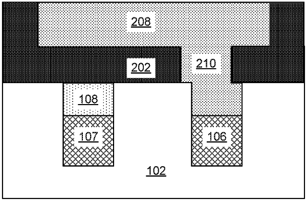
1. A method comprising:
forming a first dielectric layer, wherein the first dielectric layer includes a first conductive feature, a second conductive feature, a first polymeric feature disposed on the first conductive feature and a second polymeric feature disposed on the second conductive feature;
forming a second dielectric layer on the first dielectric layer;
forming a first trench through the second dielectric layer to expose the second polymeric feature, wherein the first polymeric feature is covered by the second dielectric layer after the forming of the first trench through the second dielectric layer to expose the second polymeric feature;
removing the exposed second polymeric feature to expose the second conductive feature, wherein the first polymeric feature is covered by the second dielectric layer after the removing of the exposed second polymeric feature to expose the second conductive feature; and
forming a third conductive feature within the first trench on the exposed second conductive feature.
|