| CPC H01F 21/12 (2013.01) [H01F 2021/125 (2013.01)] | 20 Claims |
|
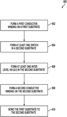
1. A method of making a slow wave inductive structure, the method comprising:
depositing a first dielectric layer over a first substrate;
forming a first conductive winding over the first substrate, wherein the first conductive winding is in the first dielectric layer;
bonding a second substrate to the first dielectric layer, wherein the second substrate is physically separated from the first conductive winding, and the second substrate has a thickness ranging from about 50 nanometers (nm) to about 150 nm;
forming a switch in the second substrate, wherein bonding the second substrate comprises electrically connecting the first conductive winding to the switch;
depositing a second dielectric layer over the second substrate; and
forming a second conductive winding over the second substrate, wherein the second conductive winding is in the second dielectric layer, the second conductive winding is electrically connected to the switch, the second substrate is physically separated from the second conductive winding, and the second substrate is between the first conductive winding and the second conductive winding.
|