| CPC G11C 7/1057 (2013.01) [G06F 13/28 (2013.01); G11C 7/1069 (2013.01); G11C 7/1084 (2013.01); G11C 7/1096 (2013.01)] | 20 Claims |
|
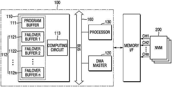
1. A memory controller comprising:
a direct memory access (DMA) master device configured to provide a first data group to a non-volatile memory device;
a program buffer memory configured to temporarily store the first data group before the DMA master device provides the first data group to the non-volatile memory device;
an exclusive OR computing circuit configured to perform an exclusive OR computation and an accumulation on a plurality of data included in the first data group provided from the program buffer memory and generate a first recovery data, after the DMA master device provides the first data group to the non-volatile memory device; and
a buffer slave device including a first program recovery buffer memory configured to store the first recovery data,
wherein the buffer slave device is connected to the DMA master device through a bus, and
the buffer slave device is configured to provide the first recovery data from the first program recovery buffer memory to the program buffer memory, in response to a program failure signal indicating that programming of the first data group on the non-volatile memory device is not completed.
|