| CPC G11C 17/18 (2013.01) [G11C 11/1673 (2013.01); G11C 17/16 (2013.01); G11C 11/161 (2013.01); G11C 11/1659 (2013.01)] | 20 Claims |
|
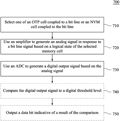
1. A circuit comprising:
an operational amplifier comprising:
an inverting input terminal capacitively coupled to each of a one-time programmable (OTP) cell array and a non-volatile memory (NVM) cell array; and
first and second output terminals;
an analog-to-digital converter (ADC) coupled to the first and second output terminals, thereby configured to receive a differential output voltage from the operational amplifier; and
a comparator coupled to the ADC and configured to output a data bit responsive to a digital output signal received from the ADC,
wherein the circuit is configured to cause the operational amplifier to generate the differential output voltage based on each of a current received from an OTP cell of the OTP cell array and a voltage received from an NVM cell of the NVM cell array.
|