| CPC G11C 16/10 (2013.01) [G11C 16/0416 (2013.01); H01L 29/788 (2013.01); H10B 43/35 (2023.02)] | 17 Claims |
|
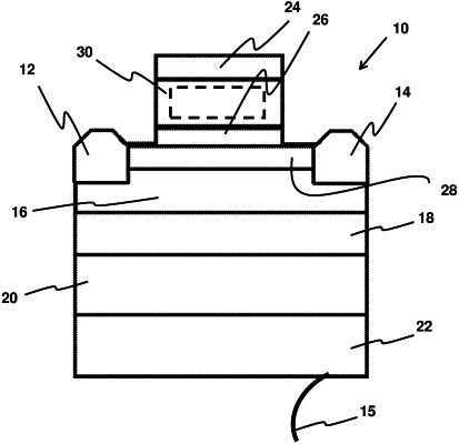
1. A memory cell for storing one or more bits of information, the memory cell comprising:
a semiconductor substrate on which is provided a source terminal, a drain terminal, and a channel extending between the source terminal and the drain terminal; and
a control gate and a floating gate, the floating gate being disposed between the control gate and the channel, and the floating gate being electrically isolated from the control gate and the channel by charge barriers and being configured to enable selective passage of charge carriers into and out of the floating gate, in write and erase operations, to provide at least first and second occupancy states of the floating gate, the channel being arranged to provide a minimum threshold voltage to be applied between the control gate and the semiconductor substrate for introducing charge carriers into the channel from the semiconductor substrate to make the channel conductive, the minimum threshold voltage being dependent on an occupancy state of the floating gate, such that a read voltage may be applied between the control gate and the semiconductor substrate that will provide a conductive channel for the first occupancy state of the floating gate and a non-conductive channel for the second occupancy state of the floating gate,
wherein an interface between the channel and the semiconductor substrate is a type-III heterojunction,
wherein the channel comprises a quantum well, a quantum dot, or a quantum wire having discrete confined energy levels for accommodating charge carriers in the channel, and
wherein a lowest confined energy level of the quantum well, the quantum dot, or the quantum wire in an absence of an electric field applied across the memory cell is at a higher energy than a valence band of the semiconductor substrate.
|