| CPC G11C 16/10 (2013.01) [G11C 16/0483 (2013.01); G11C 16/26 (2013.01); H01L 23/5283 (2013.01); H10B 41/27 (2023.02); H10B 41/35 (2023.02); H10B 41/40 (2023.02); H10B 43/27 (2023.02); H10B 43/35 (2023.02); H10B 43/40 (2023.02)] | 18 Claims |
|
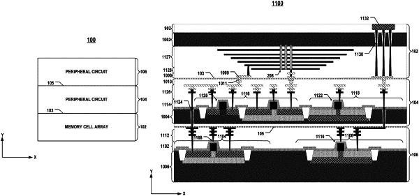
1. A three-dimensional (3D) memory device, comprising:
a first semiconductor structure comprising an array of memory cells;
a second semiconductor structure comprising:
a first peripheral circuit of the array of memory cells, the first peripheral circuit comprising a plurality of first transistors each comprising a first gate dielectric, and
a third peripheral circuit of the array of memory cells, the third peripheral circuit comprising a plurality of third transistors;
a third semiconductor structure comprising:
a second peripheral circuit of the array of memory cells, the second peripheral circuit comprising a plurality of second transistors each comprising a second gate dielectric, wherein the first and second gate dielectrics have different thicknesses, and
a fourth peripheral circuit of the array of memory cells, the fourth peripheral circuit comprising a plurality of fourth transistors; and
a first bonding interface between the first semiconductor structure and the second semiconductor structure,
wherein the first semiconductor structure, the second semiconductor structure, and the third semiconductor structure are stacked over one another, and
wherein the first transistors have a minimum operation voltage higher than a first voltage value, the second transistors have a maximum operation voltage lower than a second voltage value less than the first voltage value, and the third and fourth transistors have an operation voltage range between the first voltage value and the second voltage value.
|