| CPC G11C 16/0433 (2013.01) [G11C 7/1039 (2013.01); G11C 16/08 (2013.01); G11C 16/102 (2013.01); G11C 16/24 (2013.01); G11C 16/26 (2013.01)] | 20 Claims |
|
1. A non-volatile memory device comprising:
a memory cell array including a plurality of cell strings, each cell string extending in a vertical direction above a substrate and each cell string including a plurality of memory cells respectively connected to a plurality of word lines and a string select transistor connected to a string select line;
a page buffer circuit including a plurality of page buffers connected to the memory cell array, each page buffer including a forcing latch configured to store forcing information and each page buffer is connected to a selected cell string through a bit line; and
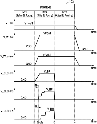
a control logic circuit configured to, during a program operation on a selected word line, control at least two of a first voltage applied to the string select line in a first interval before a bit line forcing operation for transferring the forcing information to the selected cell string through the bit line, a second voltage applied to the string select line in a second interval in which the bit line forcing operation is performed, and a third voltage applied to the string select line in a third interval after the bit line forcing operation is performed, to be different from each other.
|