| CPC G11C 11/419 (2013.01) | 20 Claims |
|
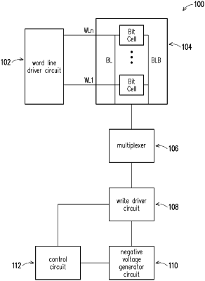
1. A memory device, comprising:
a memory cell;
a bit line connected to the memory cell;
a negative voltage generator connected to the bit line, wherein the negative voltage generator is operative to provide a first write path for the bit line;
a pull down transistor connected between the bit line and ground; and
a pull down circuit comprising a first input terminal, a second input terminal, and an output terminal, wherein the first input terminal of the pull down circuit is operative to receive data signal to be written to the memory cell, wherein the second input terminal of the pull down circuit is directly connected to the negative voltage generator and is operative to receive a write assist enable signal that is being provided to the negative voltage generator, wherein the output terminal of the pull down circuit is connected to a gate of the pull down transistor, wherein the pull down circuit is operative to enable the pull down transistor in response to the write assist enable signal attaining a second value, and wherein the pull down transistor is operative to provide a second write path for the bit line when the negative voltage generator is not enabled.
|