| CPC G11C 11/4091 (2013.01) [G11C 5/06 (2013.01); G11C 11/4074 (2013.01); G11C 11/4094 (2013.01)] | 18 Claims |
|
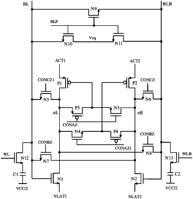
1. A sense amplifier, comprising:
an amplification circuit, arranged to read data in a memory cell and comprising a plurality of transistors; and
a control circuit, electrically connected to the amplification circuit and comprising a plurality of switches,
wherein in a first offset compensation stage of the sense amplifier, the control circuit is arranged to control, through controlling on-off states of the plurality of switches by receiving at least one control signal, the plurality of transistors of the amplification circuit to form a first inverter and a second inverter, each of the first inverter and the second inverter being an inverter with an input terminal and an output terminal connected to each other; and
in a second offset compensation stage of the sense amplifier, the control circuit is arranged to control, through controlling the on-off states of the plurality of switches by receiving the at least one control signal, a first part of the plurality of transistors of the amplification circuit to form a current mirror structure,
wherein the plurality of transistors of the amplification circuit comprise:
a first P-channel Metal Oxide Semiconductor (PMOS) transistor;
a second PMOS transistor;
a first N-channel Metal Oxide Semiconductor (NMOS) transistor, a gate of the first NMOS transistor being connected to a first bitline, and a drain of the first NMOS transistor being connected to a drain of the first PMOS transistor through a first node; and
a second NMOS transistor, a gate of the second NMOS transistor being connected to a second bitline, and a drain of the second NMOS transistor being connected to a drain of the second PMOS transistor through a second node,
wherein in the first offset compensation stage of the sense amplifier, the first PMOS transistor and the first NMOS transistor are configured as the first inverter, and the second PMOS transistor and the second NMOS transistor are configured as the second inverter.
|