|
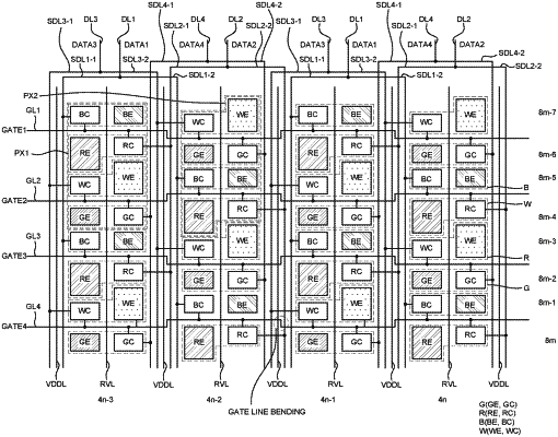
1. A display device, comprising: a display panel including a plurality of pixels, each of the plurality of pixels including a plurality of sub pixels having different colors; a data driver configured to supply a data voltage to the plurality of pixels via a plurality of data lines; and a gate driver configured to supply a gate signal to the plurality of pixels via a plurality of gate lines, wherein the plurality of sub pixels are sequentially disposed in a same column, each of the plurality of data lines is divided into two sub data lines, and the two sub data lines are disposed on opposite sides of the plurality of sub pixels disposed in the same column; wherein the plurality of sub pixels includes a first sub pixel, a second sub pixel, a third sub pixel, and a fourth sub pixel which are sequentially disposed in the same column, and wherein the first sub pixel includes a first light emitting diode and a first circuit element, the second sub pixel includes a second light emitting diode and a second circuit element, the third sub pixel includes a third light emitting diode and a third circuit element, and the fourth sub pixel includes a fourth light emitting diode and a fourth circuit element; the display device further comprising a plurality of reference voltage lines configured to sense characteristics of the plurality of pixels, wherein a corresponding reference voltage line among the plurality of reference voltage lines is disposed between the first light emitting diode and the first circuit element, between the second light emitting diode and the second circuit element, between the third light emitting diode and the third circuit element, and between the fourth light emitting diode and the fourth circuit element.
|