| CPC G09G 3/3266 (2013.01) [G09G 2300/0852 (2013.01); G09G 2310/08 (2013.01)] | 9 Claims |
|
1. A display device comprising:
a display panel having a plurality of sub-pixels thereon, the sub-pixels being connected to a plurality of scan lines and a plurality of data lines; and
a gate driver for supplying a scan signal at a high level to the plurality of scan lines,
wherein the gate driver comprises:
a first gate driver for outputting a carry signal at a low level and including a plurality of cascaded first stages;
a second gate driver for outputting the scan signal at the high level based on the carry signal and including a plurality of second stages each comprising a second output terminal connected to a respective one of the plurality of scan lines;
a first clock signal line connected to the first gate driver and the second gate driver; and
a second clock signal line connected to the first gate driver and the second gate driver,
wherein the display device comprises a start signal line connected to a top first stage among the plurality of first stages and a top second stage among the plurality of second stages, each of the plurality of first stages other than the top first stage is connected to a first output terminal of a previous one of the plurality of first stages, and each of the plurality of second stages other than the top second stage is connected to the first output terminal of the previous one of the plurality of first stages,
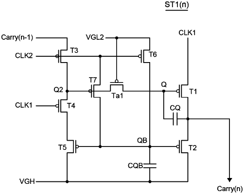
wherein each of the plurality of first stages comprises:
a first transistor having a gate electrode connected to a Q node, and a source electrode and a drain electrode connected between the first clock signal line and the first output terminal;
a second transistor having a gate electrode connected to a QB node and a drain electrode connected to the first output terminal;
a third transistor having a gate electrode connected to the second clock signal line and a source electrode and a drain electrode connected between the first output terminal of the previous first stage and a Q2 node;
a fourth transistor having a source electrode or a drain electrode connected to the Q2 node:
a fifth transistor having a gate electrode connected to the QB node;
a sixth transistor having a gate electrode connected to the second clock signal line and a drain electrode connected to the QB node; and
a seventh transistor having a gate electrode connected to the Q2 node and the Q node.
|