| CPC G09G 3/3266 (2013.01) [G09G 3/2096 (2013.01); G09G 3/3233 (2013.01); G11C 19/28 (2013.01); G09G 3/006 (2013.01); G09G 2300/0408 (2013.01); G09G 2300/043 (2013.01); G09G 2300/0842 (2013.01); G09G 2310/0286 (2013.01); G09G 2310/08 (2013.01); G09G 2330/021 (2013.01)] | 9 Claims |
|
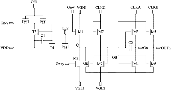
1. A detection method for a display substrate, wherein the detection method comprises:
a charging phase: controlling a cascade output terminal of a shift register in each stage to output a valid potential signal, to enable an output control circuit of the display substrate to disconnect a signal transmission with a pull-up node of a corresponding-stage shift register of the display substrate under control of a second control terminal, and to enable a detection input circuit of the display substrate to charge a first capacitor of the display substrate under control of a first control terminal and a first input terminal;
a reset phase: controlling all nodes containing the pull-up node and the cascade output terminal of the shift register in each stage to output invalid potential signals;
a discharging phase: turning on the output control circuit with the pull-up node of the corresponding-stage shift register under control of the second control terminal, and discharging only the first capacitor to the pull-up node; and
a detection phase: controlling a drive output terminal of the shift register in each stage to output a valid potential signal, providing a data voltage to at least one data signal line in a display area, detecting a voltage of a pixel electrode corresponding to the data signal line, and determining whether each of compensation sub-circuits of the display substrate is abnormal.
|