| CPC G09G 3/3233 (2013.01) [G09G 2300/0819 (2013.01); G09G 2300/0842 (2013.01); G09G 2300/0861 (2013.01); G09G 2310/0294 (2013.01); G09G 2310/08 (2013.01)] | 17 Claims |
|
1. A display device comprising:
a light emitting element; and
a pixel driving circuit connected to the light emitting element and configured to include first to fourth nodes,
wherein the pixel driving circuit includes:
a driving transistor connected to the first to third nodes;
a first transistor connected to a first scan signal line and connected between the first node and the second node;
a second transistor connected to a second scan signal line and connected between the third node and a data line;
a third transistor connected to the first scan signal line and connected between the first node and an initialization voltage line;
a fourth transistor connected to a second emission control line and connected between the second node and a first driving voltage line;
a fifth transistor connected to a first emission control line and connected between the third node and the fourth node; and
a storage capacitor disposed between the first node and the fourth node,
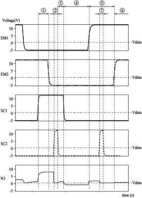
wherein a second scan signal is applied one or more times through the second scan signal line during one frame period,
wherein a time point at which the second scan signal is applied includes a first time point of applying the second scan signal and a second time point of applying the second scan signal, and
wherein a data voltage at the second time point of applying the second scan signal is a black data voltage.
|