| CPC G09G 3/3233 (2013.01) [G09G 3/2007 (2013.01); G09G 2300/0819 (2013.01); G09G 2300/0842 (2013.01); G09G 2300/0861 (2013.01); G09G 2310/0294 (2013.01); G09G 2310/08 (2013.01); G09G 2320/0247 (2013.01); G09G 2330/021 (2013.01)] | 17 Claims |

|
1. A display device comprising:
a light emitting element; and
a pixel driving circuit connected to the light emitting element and configured to include first, second, third and fourth nodes,
wherein the pixel driving circuit includes:
a driving transistor connected to the first, second and third nodes;
a first transistor connected to a first control signal line and connected to the first node and the third node;
a second transistor connected to a second control signal line and connected between the second node and a data line;
a third transistor connected to an emission control signal line and connected between the second node and a first driving voltage line;
a fourth transistor connected to the emission control signal line and connected between the third node and the fourth node;
a fifth transistor connected to a third control signal line and connected between the third node and a first initialization voltage line;
a sixth transistor connected to the third control signal line and connected between the fourth node and a second initialization voltage line; and
a storage capacitor disposed between the first driving voltage line and the first node,
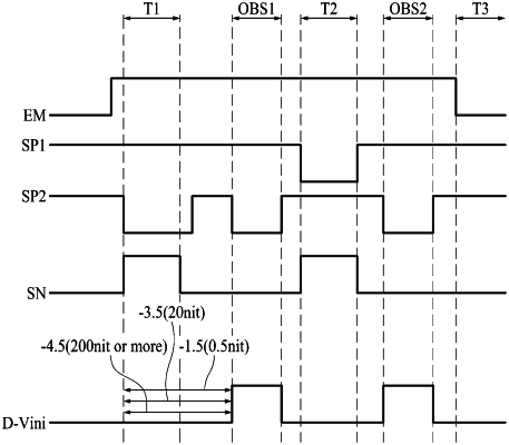
wherein the value of an initialization voltage applied through the first initialization voltage line is varied based on a data voltage applied through the data line,
wherein the pixel driving circuit is driven in an initialization period, a sampling period, and an emission period,
wherein, in the initialization period, the first control signal has a first voltage level, and the third control signal has a second voltage level lower than the first voltage level, and
wherein, after the initialization period, there is at least one on-bias stress period during which an initialization voltage is applied to the second node.
|