| CPC G09G 3/3233 (2013.01) [G09G 2300/0819 (2013.01); G09G 2300/0842 (2013.01); G09G 2300/0861 (2013.01); G09G 2330/021 (2013.01)] | 11 Claims |
|
1. An organic light emitting display device, comprising:
a display panel in which a plurality of pixels are disposed,
wherein each of the plurality of pixels includes:
an organic light emitting diode configured to emit light by a driving current;
a first transistor configured to control the driving current, the first transistor including a source electrode which is a first node, a gate electrode which is a second node, and a drain electrode which is a third node;
a second transistor configured to apply a data voltage to the first node;
a third transistor configured to form a diode connection between the second node and the third node;
a fourth transistor configured to apply an initialization voltage to the first transistor;
a fifth transistor configured to apply a high potential driving voltage to the first node;
a sixth transistor configured to form a current path between the first transistor and the organic light emitting diode;
a seventh transistor configured to apply a reset voltage to a fourth node which is an anode electrode of the organic light emitting diode; and
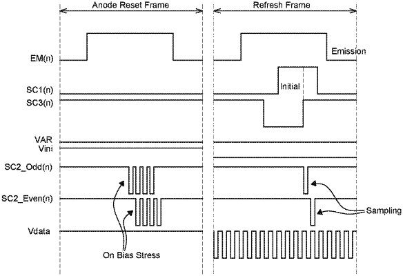
a storage capacitor including a first electrode connected to the second node and a second electrode connected to a high potential driving voltage line which transmits the high potential driving voltage, the organic light emitting display device is driven to be divided into a refresh frame when the data voltage that alternates between a plurality of different levels is programmed in the pixel and a reset frame when the anode electrode of the organic light emitting diode is reset, and the data voltage is maintained to a first level that is substantially constant during the reset frame,
wherein the second transistor includes a source electrode connected to a data line which transmits the data voltage, a drain electrode connected to the first node, and a gate electrode connected to a second scan signal line which transmits a second scan signal,
wherein the seventh transistor includes a source electrode connected to a reset voltage line which transmits a reset voltage, a drain electrode connected to the fourth node, and a gate electrode connected to the second scan signal line,
wherein during the reset frame, the second transistor is turned on by the second scan signal to apply the first level data voltage that is substantially constant to the first node and the seventh transistor is turned on by the second scan signal to apply the reset voltage to the anode electrode of the organic light emitting diode,
wherein during the refresh frame, the second transistor is turned on by the second scan signal to apply the data voltage that alternates between the plurality of different levels to the first node and the seventh transistor is turned on by the second scan signal to apply the reset voltage to the anode electrode of the organic light emitting diode, and
wherein, in all periods of the reset frame and the refresh frame, the second transistor and the seventh transistor are simultaneously turned on and simultaneously turned off.
|